As one of North America's premier technology and industrial centers, the Greater Seattle ecosystem—stretching from Bellevue and Redmond to Tacoma and Everett—has evolved beyond software leadership into a major powerhouse for hardware-software convergence, autonomous logistics, edge computing, aerospace engineering, and industrial robotics. Driven by world-class cloud hyperscalers and pioneering robotics labs, Seattle-based enterprises require highly agile Original Design Manufacturing (ODM) partners capable of translating complex optical and electronic specifications into robust, production-ready vision hardware.
In modern industrial applications, off-the-shelf camera sensors frequently fail to meet strict thermal tolerances, dynamic range demands, custom form factor constraints, and specialized interface requirements (such as MIPI CSI-2, USB 3.0 UVC, and Ethernet PHY). Our tailored ODM manufacturing service bridges this technology gap. By combining enterprise-level engineering, micro-optics active alignment, custom Printed Circuit Board Assembly (PCBA) design, and rigorous validation protocols, we empower Seattle tech companies to launch scalable hardware with unmatched time-to-market speed and optimized cost structures.
Designing vision modules specifically tuned to the environmental and computational demands of Pacific Northwest enterprises.
Seattle serves as a central hub for global e-commerce and logistics infrastructure. Our wide-angle, low-distortion camera modules equip Autonomous Mobile Robots (AMRs) and Automated Guided Vehicles (AGVs) with real-time Simultaneous Localization and Mapping (SLAM), obstacle avoidance, and high-speed pallet barcode scanning under varying warehouse illuminations.
In partnership with Seattle's expanding medical technology cluster, we engineer ultra-compact, high-definition USB and MIPI camera modules for endoscopic visual tools, automated slide scanners, and benchtop point-of-care laboratory diagnostic equipment requiring precise color fidelity and distortion-free macro focusing.
Leveraging the region's deep aerospace legacy, our robust, wide-temperature range ODM camera modules are built for airborne imaging payload platforms, UAV structural integrity inspection systems, and automated surface flaw detection systems operating in extreme flight environments.
The rapid evolution of computer vision models requires hardware that operates in sync with modern System-on-Chips (SoCs) and Edge Neural Processing Units (NPUs). Our ODM engineering roadmap addresses upcoming technical hurdles across four core development vectors:
As sensor pixel pitch decreases below 1.4µm, traditional manual optical focus techniques introduce lens tilt and field curvature errors. Our cleanroom manufacturing utilizes automated 6-axis Active Alignment (AA) equipment to adjust optical lenses relative to sensor focal planes in sub-micron increments, ensuring corner-to-corner sharp resolution across 4K and 8MP imaging modules.
To support high-frame-rate real-time AI inferencing, our hardware designs support MIPI CSI-2/CSI-3 multi-lane setups, USB 3.1 Gen2 Type-C interfaces, and GMSL2/FPD-Link III serializer/deserializer protocols capable of transmitting uncompressed 1080P/4K video feeds up to 15 meters with sub-millisecond latencies.
We integrate dedicated Image Signal Processors (ISPs) directly onto the PCBA layout, allowing hardware-level Auto Exposure (AE), Auto White Balance (AWB), High Dynamic Range (HDR up to 120dB), and distortion correction (LDC) before passing frames to host processors, significantly reducing host CPU/GPU overhead.
Supporting next-generation spatial computing and industrial inspection, our platform incorporates Near-Infrared (NIR) enhanced sensors, Short-Wave Infrared (SWIR) optics, and Time-of-Flight (ToF) depth-sensing modules optimized for dark room environments, outdoor glare, and transparent object sensing.
Executing hardware prototyping and scaling in North America often encounters long lead times, fragmented supplier networks, and high component overhead. By pairing local Seattle project management and system design with our manufacturing ecosystem in Shenzhen—the world's hub for precision electronics and micro-optics—clients benefit from an unmatchable balance of speed, cost, and agility.
From concept freeze and PCB layout to initial tooling, SMT assembly, and optical alignment sample delivery in as little as 14 to 21 business days.
Direct factory access to top-tier CMOS sensor suppliers (Sony, OmniVision, Onsemi, GalaxyCore) and optical glass element fabricators guarantees stable component availability and volume discount pricing.
Class 10,000 and Class 100 dust-free cleanrooms protect image sensor glass covers during lens bonding, preventing particle contamination that degrades image performance in industrial automated optical inspection (AOI) applications.
Deploying embedded hardware globally requires adherence to international quality standards, environmental mandates, and stringent intellectual property protections. Our ODM services incorporate end-to-end regulatory support designed specifically to simplify imports into North America and European markets:
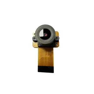
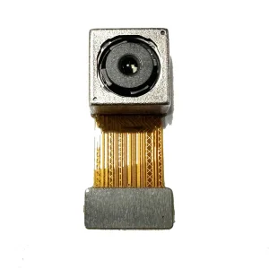
Explore our broader selection of high-definition, wide-angle, and compact camera modules engineered for seamless integration.
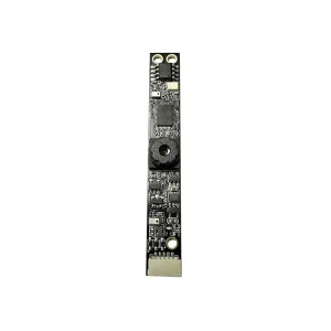
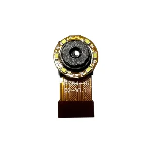
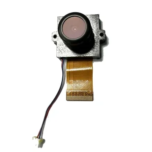
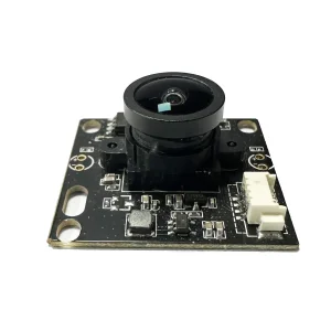
Addressing essential technical, operational, and procurement queries for engineering leads and sourcing managers.
Whether you require a low-distortion USB module, high-speed MIPI integration, or complete ground-up hardware ODM manufacturing, our engineering leadership team is standing by to assist.