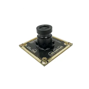
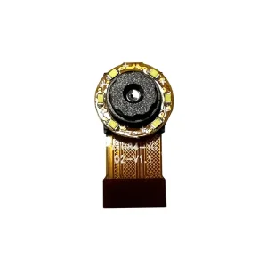
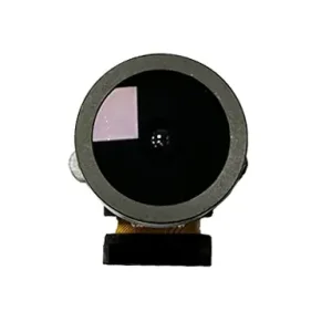
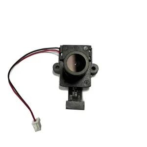
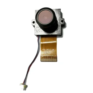
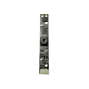
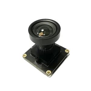
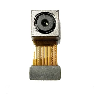
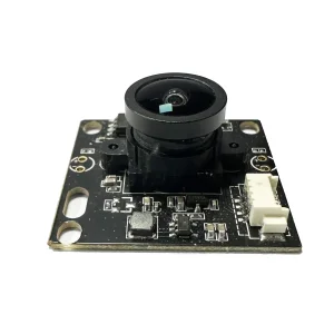
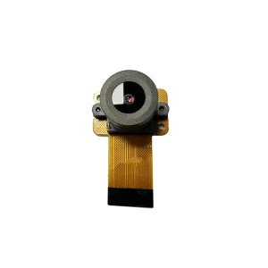
High-yield, pre-engineered optical sub-assemblies built with high MTF resolution, custom flex-PCB geometries, and wide-spectrum image signal processing.
Transitioning residential perimeter surveillance from simple passive streaming to active edge-inference intelligence. Discover how our next-generation optoelectronics reshape home security architecture.
Modern residential surveillance demands immediate spatial awareness. By embedding low-power Neural Processing Units directly on the ISP bus, our modules execute on-device human-vehicle classification, pet bounding, and gesture detection under 1.2 Watts, eradicating cloud bandwidth overhead and recurrent latency.
Overcoming the legacy monochrome infrared limitation: our modules pair large back-illuminated (BSI) pixel architectures (up to 2.0µm) with f/1.0 large-aperture hybrid glass-plastic (1G3P/2G4P) optics. This guarantees continuous color capture down to 0.001 Lux without excessive, telltale white LED spotlights.
Wide-angle residential monitoring traditionally introduces severe barrel distortion that confounds AI perimeter-tripwire algorithms. YXD manufactures custom CNC-molded aspherical elements that preserve a true 140° FoV while constraining optical edge aberration under 0.8%, maintaining pixel precision across the frame.
Architectural security challenges vary widely across residential zones. We deliver application-tailored optical assemblies fine-tuned to specific environmental constraints and data transmission protocols.
Engineered for outdoor PTZ and bullet cameras exposed to severe solar glare and inclement weather. Features include Multi-Exposure Staggered HDR (>120dB), integrated motorized ICR (Infrared Cut Filter Removable) switches rated for 300,000 cycles, and IP67 hermetic sensor potting for reliable, year-round operation.
Designed for narrow door frames and challenging lighting scenarios like bright afternoon backlighting. We configure 4:3 or 1:1 aspect-ratio portrait sensors capable of head-to-toe package monitoring, supplemented by zero-latency AEC (Acoustic Echo Cancellation) routing on integrated multi-pin interface bridges.
Balancing elderly care and infant monitoring with stringent user privacy. Modules offer localized hardware-level electronic shutter cut-offs, onboard encrypted token handshakes, and low-power PIR wakeup loops consuming under 18µA in standby mode for ultra-extended, multi-month battery life.
Headquartered in Shenzhen’s premier high-tech hardware corridor since 2015, YXD translates advanced optoelectronic design into scalable mass production with precision consistency.
Manual lens threading cannot guarantee optical center alignment across multi-megapixel sensors. We deploy 6-axis robotic Active Alignment (AA) workstations to collimate sensor and lens elements simultaneously, maintaining corner-to-corner MTF consistency across 100% of volume production batches.
Residential cameras operate uninterrupted in demanding environments. Our standard quality gate subjects every production run to continuous 48-to-72-hour thermal stress cycles (-20°C to +70°C) and elevated humidity testing, driving infant mortality rates below 50 PPM across enterprise shipments.
Direct wafer allocations from Sony, OmniVision, SmartSens, and onsemi ensure long-term availability and competitive BOM structures. Our redundant raw material staging shields enterprise buyers from supply chain disruptions, safeguarding long-lifecycle product roadmaps without unexpected redesigns.
Navigating international trade barriers, cybersecurity mandates, and privacy regulations with fully auditable, certified hardware production.
We provide verified non-blacklisted System-on-Chip (SoC) options, enabling US government-adjacent distributors and public sector contractors to maintain total regulatory compliance.
Root-of-Trust (RoT) cryptographic silicon implementation, secure boot loader validation, and randomized factory encryption credentials prevent brute-force intrusion and satisfy EU consumer standards.
Comprehensive testing for electromagnetic interference (EMI) and radiated emissions ensures clean integration alongside high-power 2.4/5GHz Wi-Fi 6 and 4G/5G cellular modules.
Direct access to Shenzhen optical architects and Linux/Android kernel engineers to assist your team with register tuning, ISP calibration, driver bring-up, and mechanical thermals.
Evaluating camera module architectures for volume residential security deployments. Match your core system specs with the optimal bus standard.
Optimal For: Edge-AI processors, battery-powered systems, Raspberry Pi 4/5, custom Linux/Android NVR carrier boards.
Core Strengths: Native zero-latency RAW bayer transmission directly into host ISP; negligible power consumption and ultra-compact FPC footprints.
Procurement Trade-Off: Shorter board-to-board cable run limits (<15-20cm without active SerDes serializers).
Optimal For: Smart access terminals, indoor intercom screens, all-in-one desktop devices, automated file verification consoles.
Core Strengths: True cross-platform plug-and-play across Windows, Android, and Ubuntu without custom driver compilation.
Procurement Trade-Off: Host-side compression overhead (MJPEG/H.264/H.265) necessary for 4K streaming over USB 2.0 lines.
Optimal For: Wireless solar yard security cameras, portable battery video bells, plug-in consumer perimeter monitors.
Core Strengths: Complete embedded board layout with system-on-chip, memory, radio module, and cloud p2p streaming protocol support.
Procurement Trade-Off: Requires robust on-board RF isolation engineering and regional antenna certification compliance.
Key considerations for hardware procurement leads, product line managers, and optical engineers.
For standard sensor configurations with existing optical designs, functional evaluation samples are typically dispatched within 7–10 business days. When full custom engineering is required—including custom multi-layer Rigid-Flex FPC layouts, specialized M12/M8 lens barrel machining, or unique IR pass filter coatings—sample delivery ranges from 20 to 25 business days, including complete optical simulation files and MTF test documentation.
We work closely with primary tier-one silicon foundries (Sony, OmniVision, onsemi, SmartSens) to secure continuous wafer allocations. We provide enterprise customers with transparent lifecycle tracking and minimum 6-to-12-month advance notifications of silicon transitions, accompanied by pin-compatible alternate layout paths and driver update support to prevent field disruptions.
Yes. Our in-house optical software team specializes in low-level register and ISP calibration. We customize auto-white balance (AWB), auto-exposure curves (AEC), 2D/3D noise reduction matrices, and wide dynamic range (WDR) settings for difficult backlighting, infrared night illumination, or mixed-spectrum environments.
Sample stages for design qualification support small batches starting from 10 to 50 units. For mass production runs, standard MOQs begin at 1,000 units per scheduled batch. With multiple automated SMT and robotic Active Alignment cleanroom lines, our total monthly assembly capacity exceeds 600,000 finished camera sub-assemblies.
Outdoor-rated assemblies undergo rigorous pressure-decay testing to verify IP66/IP67 compliance, alongside thermal cycling in environmental test chambers operating from -40°C to +85°C. We utilize structural adhesives and UV-cured optical sealants with minimal outgassing properties, preventing internal lens fogging and focus shifts across seasons.
Ready-to-deploy imaging modules covering high-speed driving logs, building access panels, and high-resolution industrial monitoring applications.