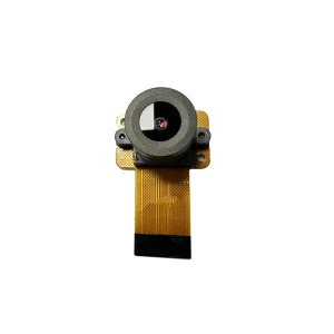
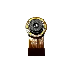
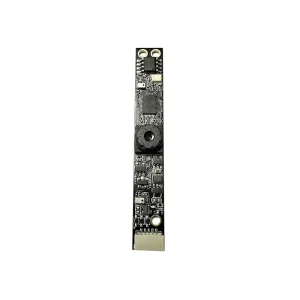
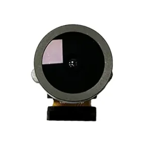
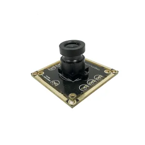
High-precision sensor integration and custom focal length lenses engineered to capture biometric facial landmarks under complex ambient illuminations.
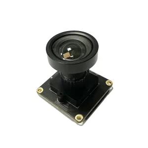
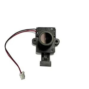
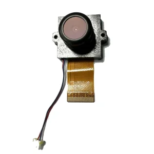
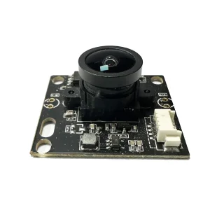
Facial biometric accuracy relies on the optical integrity of input frames. Our factory bridges sensor physics, ISP firmware customization, and precision lens fabrication to meet stringent modern identification benchmarks.
Modern face verification demands dual-spectrum sensing. We construct dual-lens RGB + NIR (Near Infrared) synchronization modules that extract 3D depth landmarks and thermal vascular signatures, neutralizing 2D paper, tablet, and curved silicon mask attacks at the edge.
Facial feature vector extraction relies on accurate spatial distance ratios between pupils, nasal bridges, and cheekbones. Our in-house SMT and optical tooling yield TV distortion rates below 0.5%, avoiding peripheral warping common in generic wide-angle lenses.
Real-world face recognition terminals face direct sunlight, building reflections, and pitch-black nocturnal conditions. Our sensor arrays feature multi-exposure staggered WDR, resolving overexposed skylights and dark shadow zones concurrently.
Situated at the hub of global optoelectronic manufacturing, Shen Zhen You Xiang Da Technology Co., Ltd. (YXD) leverages cleanroom automation, component clusters, and supply agility to lower B2B procurement risk.
Immediate access to leading CMOS wafer suppliers (Sony, OmniVision, Onsemi) and rapid glass-plastic lens molding hubs in the Pearl River Delta cuts prototype lead times down to 7-10 days.
COB (Chip-on-Board) and SMT production lines are housed inside dust-free facilities to avoid pixel contamination, maintaining pristine modulation transfer function (MTF) yield curves.
Every camera batch undergoes burn-in aging chambers, high-low temperature shock cycles (-30°C to +75°C), and automated MTF chart validation before shipment.
Our in-house R&D customizes sensor registers, ISP auto-exposure (AE) weighting routines, and UVC descriptors to suit your chosen Linux, Android, or ROS deployment.
Selecting the optimal interconnect bus establishes edge processing efficiency, bandwidth utilization, latency bounds, and cable transmission limits.
| Protocol Interface | Host System Fit | Effective Bandwidth | Transmission Distance | Biometric Image Latency | Recommended Vision Scenario |
|---|---|---|---|---|---|
| MIPI CSI-2 (2/4 Lane) | Rockchip, NXP, Jetson, Raspberry Pi | Up to 2.5 Gbps per lane | Short FPC (< 20 cm) | Ultra-Low (< 15 ms direct DMA) | High-throughput edge AI face recognition boxes |
| USB 2.0 / 3.0 UVC | Windows, Linux, Android, macOS | 480 Mbps (USB2) / 5 Gbps (USB3) | Up to 3-5m (Copper) | Low (30-50 ms with MJPEG/YUY2) | Commercial kiosks, e-gates, access terminals |
| DVP Parallel | Low-power microcontrollers (STM32, ESP32) | Up to 100 Mbps | Ultra-short (< 10 cm PCB) | Low (Resolution dependent) | Cost-sensitive smart locks, attendance scanners |
| Wi-Fi / Ethernet IP | Cloud platforms, NVRs, Network gateways | Varies by network protocol | Local network / Worldwide | Medium (100-300 ms H.264/H.265 stream) | Building security, distributed smart perimeter monitoring |
Explore how optical sensor customization resolves edge recognition challenges across major industry verticals.
Airport security turnstiles and office towers demand sub-second matching as users approach. Our wide-angle, low-distortion modules integrate automatic ISP exposure switching to recognize tall and short visitors equally without physical motor tilt adjustments.
Cash dispensers and unattended payment machines require high-level optical anti-spoofing certification. By pairing 850nm/940nm narrowband IR bandpass filters with tailored RGB chromatic sensors, our units stop printed and phone-screen presentation attacks.
Automotive Driver Monitoring Systems (DMS) identify driver fatigue, eye closures, and unauthorized operators. We supply compact starlight and global-shutter camera modules that maintain sharp tracking through sunlight, shadows, and darkness.
Avoid project delays and redesign loops. Review our 5-step engineering engagement model from optical design validation to full-scale mass assembly.
Evaluation of Field of View (DFOV/HFOV), sensor target format (1/2.7", 1/3"), target resolution (1080P, 4MP, 4K), illumination spectrum requirements, and terminal physical dimensional limitations.
Custom PCB design with tailored FPC pinouts (e.g., standard 15-pin/22-pin Raspberry Pi or custom board-to-board connectors), paired with Zemax optical simulations to verify MTF corner sharpness.
Rapid CNC module sample production within 7-10 business days. Direct ISP color matrix, gamma curve, auto-exposure, and anti-flicker calibration matched to your target operational illumination.
Prototypes are tested in thermal aging vaults, mechanical vibration fixtures, and humidity chambers, verifying zero optical defocus or glue detachment across long duty cycles.
Batch fabrication using automated active alignment (AA) machines. Every module is indexed with barcode traceability, lens focus locking, and clean packaging for global delivery.
Direct allocations with sensor wafer fabs provide multi-year chipset longevity roadmaps, shielding industrial clients from sudden EOL component surprises.
Review additional production-ready models including ultra-wide angle, miniature 9mm form factors, and autofocus optical modules.
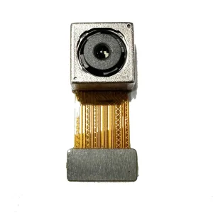
Key technical and commercial answers directly from our factory engineering team.