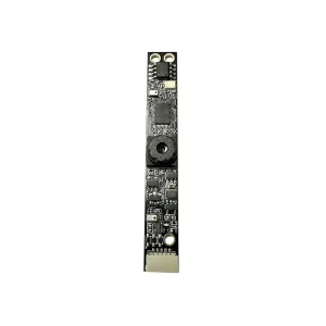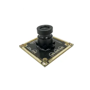
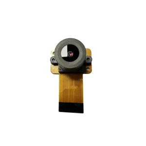
Field-proven camera architectures designed for edge biometric ingestion, surveillance verification, and dynamic intelligent access systems.
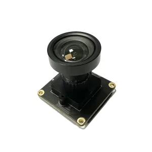
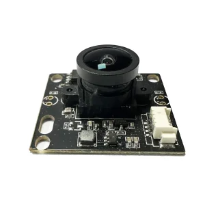
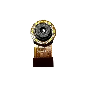
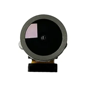
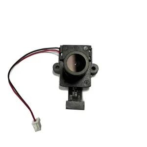
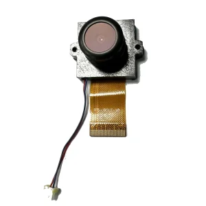
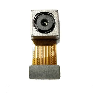
Transitioning from basic 2D image matching to multi-spectral, privacy-compliant, edge-computed neural biometric ecosystems.
Traditional cloud-dependent facial matching architectures suffer from latency bottlenecks and bandwidth cost overruns. Modern programs deploy quantized convolutional neural networks directly onto edge NPUs, delivering match latency under 150ms while isolating raw biometric data locally.
Presentation attacks (print photos, curved high-resolution screens, 3D silicone masks) render legacy single-lens RGB recognition obsolete. Integrated dual-band systems capture synchronized visible light and near-infrared (850nm/940nm) to calculate genuine sub-surface dermal reflectance.
Industrial access points and electronic gates are migrating rapidly toward Time-of-Flight (ToF) and structured light optics. By superimposing 30,000+ invisible infrared dots, the facial program constructs sub-millimeter geometric point clouds immune to ambient illumination extremes.
Enterprise procurement teams must balance bus bandwidth, ISP computational offloading, and physical chassis thermal dissipation.
| Architecture Protocol | Optimal Distance & Application | Processor / SoC Requisites | System Bandwidth & Latency | Liveness Detection Suitability |
|---|---|---|---|---|
| MIPI CSI-2 Dual-Lane | 0.3m – 1.8m (Turnstiles, Embedded Biometric Terminals) | ARM Cortex-A55 / Rockchip RK3588 / NXP i.MX8M with hardware ISP | Raw sensor stream up to 2.5 Gbps/lane; Zero protocol conversion overhead; <10ms glass-to-memory | Optimal Directly syncs RGB + IR sensors on shared MIPI bus for microsecond liveness correlation. |
| USB 2.0 / USB 3.0 UVC | 0.5m – 3.0m (Interactive Kiosks, Self-Service ATMs, POS) | x86_64, Linux, Android, Windows Host running standard V4L2 or DirectShow | 480 Mbps (USB 2.0 MJPEG) to 5 Gbps (USB 3.0 YUV uncompressed); Driver-free plug-and-play integration | High Requires hardware synchronization between dual sensor USB bridges or composite video devices. |
| DVP Parallel Interface | 0.2m – 0.8m (Cost-Constrained Time Attendance Terminals) | Low-power RTOS microcontrollers (STM32, ESP32-S3) with parallel camera interface | Bandwidth limited to VGA / 720P @ 15-30fps; Highly economical PCB tracing and bill-of-materials | Moderate Suitable for baseline 2D authentication; constrained processing overhead for 3D depth maps. |
| IP / Ethernet (RTSP/ONVIF) | 2.0m – 15m (Enterprise Video Surveillance, Perimeter Flow) | Standalone Network Video Recorder (NVR) or Cloud-Edge Hybrid Compute Matrix | H.264/H.265 compressed streams; 50-250ms network transport latency depending on RTSP buffer | Selective Dependent on far-field edge analytics; primarily operates on 2D visible features under high dynamic range. |
Customizing optical tuning, illumination spectral arrays, and edge algorithms across mission-critical application domains.
Equipped with wide dynamic range (WDR > 120dB) CMOS sensors, preventing face washouts in extreme morning glare or backlighting behind glass office vestibules. Fully integrated with optical anti-distortion elements to preserve aspect ratio accuracy along frame perimeters.
Unattended payment kiosks require zero-friction authentication combined with financial-tier anti-fraud thresholds. Dual-sensor RGB+NIR modules eliminate spoofing by static prints or 4K tablet screens while maintaining sub-second validation across diverse ethnic demographics.
Automotive grade driver monitoring systems (DMS) demand high-speed global shutter sensors to counter optical motion blur during vibration. Near-infrared pulsed illumination guarantees face identification and drowsiness tracking through polarized sunglasses and nighttime environments.
Shenzhen engineering excellence meeting stringent North American and European regulatory frameworks.
Our facial recognition program architectures emphasize localized edge computation where raw mathematical vector embeddings (hashes) are processed in volatile memory. No plain image streams need persistent storage, enabling full compliance with global biometric privacy laws.
For defense, aerospace, and municipal infrastructure procurement, we provide non-restricted semiconductor BOM options. Sensor arrays and microcontrollers can be customized using Sony, OmniVision, and Western-compliant ISP platforms to satisfy global trade import requirements.
Outdoor access terminals face wide temperature deltas. YXD modules undergo 72-hour thermal stress cycles (-20°C to +70°C), verifying that adhesive active alignment (AA) between lens optics and CMOS image sensor does not suffer focal plane drift or optical MTF drop.
Anticipating structural engineering shifts across photonic hardware, neuromorphic vision, and encrypted biometric silicon.
Integrating asynchronous event sensors that trigger data output only when pixel-level illumination fluctuates. This yields ultra-low power consumption (<10mW standby) and dynamic ranges exceeding 140dB, revolutionizing battery-powered residential smart locks and wearable terminals.
Embedding hardware cryptographic root-of-trust directly within the CMOS sensor substrate. Raw pixel registers are encrypted at the moment of photon collection, ensuring that MIPI physical bus intercept attacks (man-in-the-middle sniffing) fail completely at the physical board trace level.
Advancing into Short-Wave Infrared (1050nm to 1550nm) spectrum monitoring. This enables the verification of active human blood vessel oxygenation and moisture levels alongside facial geometric structures, rendering spoofing via silicon prosthetics physical impossibilities.
In-depth engineering answers addressing OEM integration, optics customization, and computational pipelines.
Industrial imaging modules engineered for extreme environments, miniature enclosures, and low-distortion document/biometric digitization.